PCB Fabrication Steps
STEP – 1: PREPARING THE ARTWORK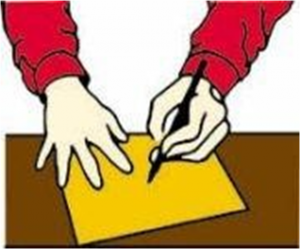
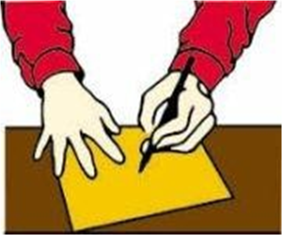
Firstly design the required circuit. The best option is to design the circuit on a computer and print or plot a 1:1 artwork onto a translucent or transparent film. Ideally print the artwork via a Laser printer. If the software allows print a mirror image of the circuit as this will ensure the black areas of the artwork will be in contact to the PCB’s Photoresist during UV exposure.
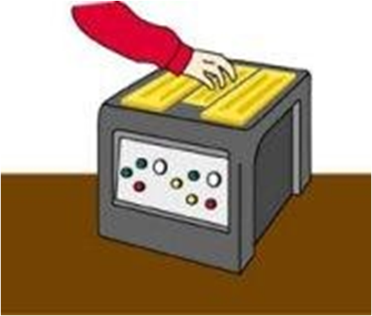
STEP – 2: EXPOSING PRINT ON pH PCB
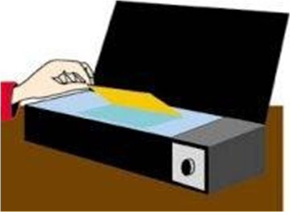
Select a suitable piece of CCB with pH (Photoresist) Coating. pH PCB Can be made by using Dry Film Laminator by laminating dry film on CCB. If necessary cut a piece using a suitable shear. Remove the
protective black plastic from the pH CCB to reveal the photoresist. Position the artwork in contact with the photosensitive side of the pH CCB and place both in the UV exposure unit, artwork down. Having closed the lid set the unit’s integral timer to the correct time and the exposure will automatically commence.
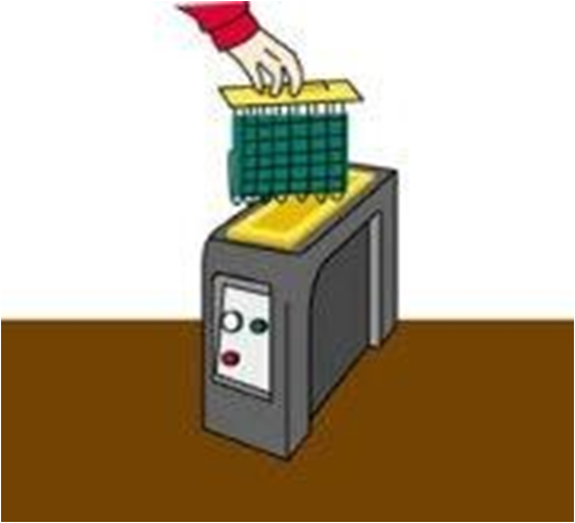
STEP – 3: DEVELOPING THE IMAGE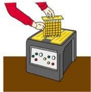

Place the board to be developed in Tank board holder and immerse in the developing tank. This along with the quality of the artwork and UV unit is the most critical part of PCB production. It is very important to
ensure the board is not over-developed. The developed image can look good, but over-developing can cause a reduction in the thickness of the resist, which could then break down at the etching stage. A 20 : 1 dilution with water for Developer should be sufficient. Developers with the photoresist used on pH CCB can be used a room temperature without heating. When developing, remove and wash after 15—30 seconds. If the board needs a little more evelopment, then immerse into the developer for a few more seconds and then wash immediately gain.
STEP – 4: SPRAY WASHING
Use the Spray Wash Tank immediately after the board is removed from the Developer. For washing we can use Distilled Water for fine cleaning.
STEP – 5: ETCHING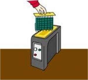
The developed and washed board is then placed into the Etching Tank. The board is placed in the lid / basket holder and immersed into the etchant, with the lid on the Air Pump is turned on and at normal etching temperature of 45 ºC for ferric etching should take approximately 5 minutes.
STEP – 6: RESIST STRIPPING
The PCB will now consist of an etched circuit still covered in the photoresist. This can be removed with the resist strip applicator in Tank. As before the lid/board holder is raised at any time to examine the board. The photoresist should be stripped off in approximately 2-3 minutes. Once the photoresist has been stripped from the circuit the board holder and board are then spray washed.
STEP – 7: SCRUB CLEANING

The board is then thoroughly dried and mechanically scrubbed with scrub pad. This will ensure that the copper circuit is perfectly clean by removing any oxidisation, passivation or chlorides left by the water as well as any other impurities. After scrubbing, any small particles left by the silica block should be wiped off with a clean dry tissue.
STEP – 8: TIN PLATING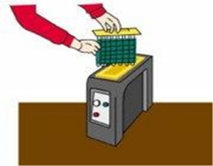

Before the clean board has had a chance to oxidise again it should be immersed Tin solution for 7-15 minutes. Once immersed in the solution this unique tin which operates at low temperature will begin to work immediately and plate a very smooth surface of small molecules of tin onto the copper circuit. This will stop the copper from oxidising and will also act as a solder flux. For best results when you remove the board from the tin solution immerse immediately in cold water then rinse thoroughly in hot and wipe dry with a paper towel.